Semiconductor Packaging Market Growth, Key Segments, and Regional Dynamics with Manufacturers and Suppliers Data
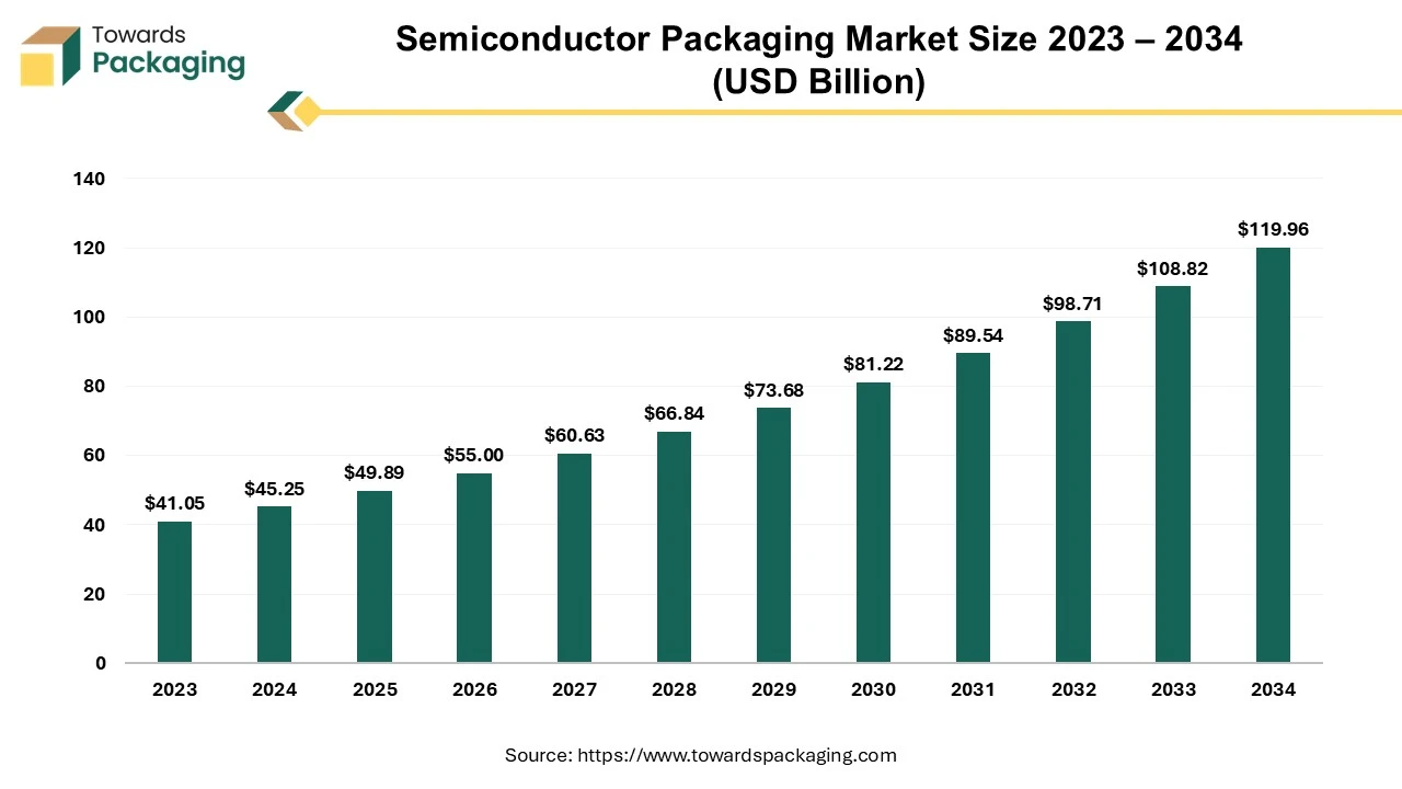
As reported by Towards Packaging experts, the global semiconductor packaging market is anticipated to rise from USD 55 billion in 2026 to approximately USD 119.96 billion by 2034, with a CAGR of 10.24% from 2025 to 2034.
Ottawa, Nov. 04, 2025 (GLOBE NEWSWIRE) — The global semiconductor packaging market, valued at USD 49.89 billion in 2025, is expected to rise to approximately USD 119.96 billion in 2034, based on a report published by Towards Packaging, a sister firm of Precedence Research. The semiconductor packaging market is vital to modern electronics, as it protects the fragile chip, connects it to other components, and significantly affects its performance, reliability, and even power efficiency.
Request Research Report Built Around Your Goals: sales@towardspackaging.com
What is Meant by Semiconductor Packaging?
Semiconductor packaging is the procedure of enclosing a bare silicon chip in a protective case to cover it from physical damage, moisture, and even contamination, while also offering the electrical connections required to integrate it into a larger electronic apparatus. The package is programmed to be a path for heat to escape the chip, and to prevent overheating along with ensuring reliable performance. Thus, its material and structure are vital for thermal management.
What are the Major Government Initiatives in the Semiconductor Packaging Industry?
- U.S. CHIPS and Science Act (specifically the National Advanced Packaging Manufacturing Program – NAPMP): This U.S. initiative provides significant direct funding and tax credits to establish a robust domestic advanced packaging ecosystem. It aims to accelerate the transfer of advanced packaging innovations from research to manufacturing and develop a skilled workforce to ensure U.S. competitiveness in high-performance computing and AI.
- India Semiconductor Mission (ISM) – ATMP/OSAT Scheme: As part of a comprehensive program with a total outlay of ₹76,000 crore, this scheme offers substantial fiscal support of up to 50% of capital expenditure for eligible applicants setting up Assembly, Testing, Marking, and Packaging (ATMP) or Outsourced Semiconductor Assembly and Test (OSAT) facilities. This initiative aims to build a complete domestic semiconductor value chain, reduce import dependence, and position India as a global manufacturing hub.
- European Chips Act (specifically the APECS Pilot Line): The EU Chips Act includes a “Chips for Europe Initiative” that funds advanced pilot lines, such as the APECS (Advanced Packaging and Integration for Electronic Components and Systems) pilot line led by Fraunhofer in Germany. This pan-European effort focuses on R&D and prototyping for advanced heterogeneous integration and chiplet technologies, bridging the gap between lab research and commercial production to enhance the EU’s technological autonomy.
- China’s National Integrated Circuit Industry Investment Fund (Big Fund): While not a single act with a simple name, China’s extensive state-backed funding mechanisms, including the “Big Fund,” have heavily subsidized the development of its domestic semiconductor industry, including advanced packaging capabilities. These efforts aim to achieve self-sufficiency in semiconductor production as part of national strategic goals like “Made in China 2025” and reduce reliance on foreign technology amidst geopolitical tensions.
- Japan’s Semiconductor Strategy (involving Rapidus and JSR): Japan is fostering domestic semiconductor manufacturing and packaging through initiatives involving public-private partnerships, such as supporting the new venture Rapidus to produce cutting-edge logic chips. The government is also investing in key materials suppliers and promoting R&D collaborations to build a resilient and innovative semiconductor ecosystem.
Get All the Details in Our Solutions – Access Report Sample: https://www.towardspackaging.com/download-sample/5221
What are the Latest Trends in the Semiconductor Packaging Market?
Advanced Materials and Bonding Techniques
They are necessary to overcome the restrictions of conventional packaging, permitting higher performance, miniaturization, and even power efficiency required by modern applications such as AI, 5G, and IoT. Consumer electronics and a few devices need smaller form factors. Advanced packaging permits multiple chips to be combined into a single package, and even fitting more functionality into a smaller space. As chips become more powerful, they cause more heat. Advanced packaging materials and even designs are designed to dissipate this heat more effectively, guaranteeing components function within their optimal temperature range.
Use of AI in Packaging Design for Process Optimization
Due to the rising complexity and even demands of modern chips. To manufacture smaller, faster, and even more energy-efficient chips for applications such as AI, 5G, and high-performance computing, the industry must overcome remarkable challenges in manufacturing efficiency, expense, and reliability.
Semiconductor manufacturing includes hundreds of precise steps, with packaging becoming a key function rather than a secondary one. AI algorithms process information from IoT sensors on production equipment to monitor and even automatically correct process parameters. This transition from reactive to autonomous control improves throughput and decreases variations in quality.
What Potentiates the Growth of the Semiconductor Packaging Industry?
Proliferation of Emerging Technologies
By creating a need for more powerful, compact, and even energy-efficient chips that traditional packaging methods cannot support. Advanced technologies such as artificial intelligence (AI), 5G, and even the Internet of Things (IoT) push the restricts of chip performance, miniaturization, and also integration, demanding sophisticated packaging solutions to protect and allow these complex electronic components.
Meanwhile, AI development also drives the usage of heterogeneous integration and even chiplet-based architectures, where multiple specialized chiplets are combined into a single package to boost performance. As power density raises in high-performance chips, innovations in packaging materials and even designs for cooling become critical for reliability.
Limitations & Challenges
It includes high expenses for advanced technologies, complex thermal and even signal integrity management for smaller, denser chips, supply chain issues such as material scarcity and geopolitical tensions, and even increasing environmental along regulatory hurdles. In addition, the rising complexity of integrated circuits (ICs) makes testing and even ensuring reliability more difficult.
Advanced packaging needs substantial investment in R&D, along with specialized equipment and even manufacturing facilities, which can be a barrier for smaller firms. The usage of hazardous chemicals and even high energy consumption in manufacturing contributes to significant compliance expenses and environmental risks.
Elevate your packaging strategy with Towards Packaging. Enhance efficiency and achieve superior results – schedule a call today: https://www.towardspackaging.com/schedule-meeting
Regional Analysis
Who is the Leader in the Semiconductor Packaging Market?
Asia Pacific leads the market because of advanced manufacturing infrastructure, massive consumer electronics demand, and significant government support. A massive user base with growing disposable incomes fuels the need for smartphones, laptops, and other apparatus, which are major users of packaged semiconductors. Taiwan’s early and heavy government investment in the 1970s made it a strategic advantage, while a few nations also actively invest to decrease reliance on foreign solutions.
China Market Trends
China’s market is driven by the need for AI, 5G, and even electric vehicles (EVs), leading to a rapid growth in advanced packaging technologies such as 3D and flip-chip. Key trends involve a shift from volume-driven to performance-based packaging, rising R&D investment by domestic manufacturers, and even policy support for technological self-sufficiency.
Japan Market Trends
Japan’s market is undergoing significant growth, with a projected CAGR of nearly 10-12.5% through 2030-2033, pushed by need in consumer electronics, telecommunications, and automotive. Ceramic packages are favored for high-performance applications because of their thermal conductivity, and even advances in die attach materials are also driving growth.
How is the Opportunistic Rise of North America in the Semiconductor Packaging Industry?
This is driven by significant government incentives, a high need for advanced packaging, and even a push for greater supply chain resilience. The U.S. CHIPS and Science Act offers substantial funding and incentives to drive domestic semiconductor manufacturing and even advanced packaging capabilities. This has supported new back-end factories in states such as Arizona and New Mexico and is even directly driving market expansion.
U.S. Market Trends
The U.S. market is experiencing remarkable growth driven by AI, 5G, and even the expansion of advanced technologies such as 3D packaging, SiP, and FOWLP. The consumer electronics, along with the automotive sectors, are leading need, while other areas such as data centers and IoT are also leading to market expansion.
Traditional packaging materials like organic substrates still dominate revenue, but the fastest-growing segments are wire bonding and advanced platforms. On the technology front, formats such as fan-out wafer-level packaging (FOWLP), 2.5D/3D integration, and system-in-package (SiP) are being rapidly adopted, driven by demands for higher bandwidth, lower latency, and heterogeneous integration of chiplets.
More Insights of Towards Packaging:
- Active Packaging Market Size, Segments, Companies, Competitive Analysis, Value Chain & Trade Analysis 2025-2034
- Bulk Container Packaging Market Size, Segments and Regional Outlook 2025–2034
- Connected Packaging Market Size, Segmentation, Regional Outlook, and Competitive Landscape, 2025-2034
- Nanotechnology Packaging Market Size, Share, Trends, Segmentation, Regional Outlook
- Form-Fill-Seal Packaging Market Size, Segments Data, and Regional Insights
- Packaging 4.0 Market Size, Segments Data, and Competitive Analysis
- Packaging Automation Market Size, Segmentation, Regional Insights
- Packaging 5.0 Market Trends, Segments, Regional Performance
- Cold Chain Packaging Refrigerants Market Size, Segments, Regional Data
- Packaging Machinery Market Size, Segments, and Regional Analysis
- Labeling Machine Market Growth, Key Segments, and Regional Dynamics
- Cold Chain Packaging Market Size, Segments, Regional Insights
- Packaging in Supply Chain Management Market Size, Segments Data
- Automotive Packaging Market Size, Segments, Regional Outlook
- Smart Packaging Market Size, Share, Segments, Regional Outlook
- Intelligent Packaging Market Size (2025-2034), Segments, Regional Outlook
- AI in the Packaging Market Size, Segmentation, Regional Outlook
Segment Outlook
Material Type Insights
Why did the Organic Substrate Segment Dominates the Semiconductor Packaging Market in 2024?
This is due to its cost-effectiveness along with versatility, which makes it an economical option for the high-volume consumer electronics market. Meanwhile, organic substrates are a cheaper option to materials such as ceramics, which is vital for the high-volume production needed by the consumer electronics sector. Continuous research and even development are contributing to enhancements in organic substrate materials, allowing their usage in more advanced applications such as high-speed signaling and heterogeneous integration.
The bonding wire segment is the fastest growing in the market, due to its cost-effectiveness and versatility, boosted by the increasing need for advanced, miniaturized chips in automotive, consumer electronics, and IoT applications. Advancements in materials such as copper and silver, together with automation, are making it a more attractive option than more expensive solutions while managing reliability. The growth of IoT devices creates a massive need for a variety of semiconductor components that usually rely on cost-effective and even versatile bonding wire solutions. Silver has also become a famous and viable option for applications such as LED and memory devices, providing similar performance to gold at a lower price point.
Technology Type Insights
Why did the Traditional Packaging Segment Dominates the Semiconductor Packaging Market in 2024?
This is due to its cost-effectiveness and even established reliability, mainly in high-volume consumer electronics and also automotive applications. Its long history has resulted in proven, large-scale production processes, making it the most economical and proven choice for many applications. Traditional packaging, thus, holds the largest revenue share because of its massive volume in these core industries, as well as advanced packaging continues to expand rapidly.
The advanced packaging segment is the fastest-growing in the market, due to the increasing need for smaller, higher-performance, and even more power-efficient chips to permit technologies such as 5G, AI, and IoT. Advanced packaging enables the incorporation of multiple chips into a single package, decreasing size and power consumption while boosting performance, which is vital for modern consumer electronics, autonomous vehicles, and a few next-generation devices. Advanced packaging permits heterogeneous integration, where different kinds of chips are combined in one package. This approach enhances performance, reduces expenses by using fewer discrete components, and improves manufacturing efficiency.
End Use Insights
Why did the Consumer Electronics Segment Dominates the Semiconductor Packaging Market in 2024?
This is due to the high volume of chips needed for products such as smartphones and laptops, which require advanced packaging solutions for miniaturization, energy efficiency, and higher performance. Devices such as smartphones, tablets, and even wearables are manufactured in massive quantities, creating a vast and even consistent demand for semiconductor chips and their packaging. Every new generation of consumer electronics targets to be faster and more capable. This involves integrating more features such as AI, higher-resolution cameras, and even faster connectivity, which necessitates advanced packaging to fund high-performance chips.
The aerospace & defence segment is the fastest-growing in the market, due to the increasing demand for high-reliability, solid packaging solutions for advanced military and even civilian aerospace applications. Modern warfare, along with aerospace applications, needs advanced electronics for communications, radar, and electronic warfare, which in turn drives the need for high-performance, miniaturized, and even energy-efficient semiconductors. Rising worldwide defense budgets and even a strategic focus on securing domestic semiconductor supply chains contribute to increased investment in advanced packaging technologies.
Recent Breakthroughs in the Global Semiconductor Packaging Industry
- In August 2025, Amkor Technology, Inc. declared revised plans for the location of the firm’s new semiconductor advanced packaging and even test facility in Arizona. The facility will now be constructed on a 104-acre site, within the Peoria Innovation Core. The Peoria City Council unanimously accepted a land swap and even an amended development agreement, permitting Amkor to exchange its previously engineereed 56-acre parcel within the Five North at Vistancia community.
- In January 2025, $1.4 billion was announced by the U.S. Department of Commerce in final awards. This fund was expected to support the next generation of U.S. semiconductor advanced packaging and new technology validation.
Top Companies in the Semiconductor Packaging Market
- HCL Technologies: HCL Technologies provides semiconductor packaging design and qualification services as part of its broader silicon engineering solutions for clients, rather than offering in-house, high-volume manufacturing.
- Moschip Semiconductor Technologies: Moschip is a semiconductor and system design services company that focuses on turnkey ASICs and IP development, partnering with external foundries for manufacturing and implicitly involving packaging expertise within its design solutions.
- SPEL Semiconductor: SPEL is an Outsourced Semiconductor Assembly and Test (OSAT) vendor in India, providing full turnkey solutions including wafer sort, assembly (packaging), testing, and drop-shipment services.
- Ruttonsha International Rectifier Ltd (now RIR Power Electronics): The company primarily manufactures power semiconductor devices and equipment (like diodes, rectifiers, thyristors) and is establishing a Silicon Carbide plant, with packaging being an integrated part of its power device manufacturing process.
- ASE (ASE Technology Holding Co., Ltd.): ASE is a global industry leader and major Outsourced Semiconductor Assembly and Test (OSAT) provider, offering a comprehensive range of advanced semiconductor packaging and testing services.
- Amkor Technology: Amkor is a leading global provider of outsourced semiconductor packaging and test services, designing, packaging, and testing integrated circuits for chip manufacturers worldwide.
- JCET Group: JCET Group is a prominent global semiconductor assembly and test provider, offering a wide range of packaging and testing solutions, including advanced packaging technologies.
- Siliconware Precision Industries Co., Ltd. (SPIL): SPIL is a major player in the global market, specializing in semiconductor packaging and testing services as an independent outsourced provider.
- Powertech Technology Inc. (PTI): PTI is an important Outsourced Semiconductor Assembly and Test (OSAT) company that provides memory and logic integrated circuits packaging and testing services.
- Tianshui Huatian Technology Co., Ltd.: Huatian Technology is a significant Chinese OSAT company offering a broad portfolio of semiconductor assembly and test services.
- Fujitsu Semiconductor Ltd.: Fujitsu Semiconductor focuses on the design and manufacture of its own semiconductor products, including microcontrollers and power devices, and does not operate as a third-party, general-purpose OSAT service provider in the same way as the other dedicated packaging companies listed.
Segments Covered in the Report
By Material Type
- Bonding Wire
- Organic Substrate
- Ceramic Package
- Leadframes
- Encapsulation Resins
- Die Attach Material
- Thermal Interface Materials
- Solder Balls
- Others
By Technology Type
- Advanced Packaging
- Flip Chip
- Embedded Die
- 5D/3D
- SIP
- Fan-in Wafer Level Packaging (FI-WLP)
- Fan-out Wafer Level Packaging (FO-WLP)
- Traditional Packaging
By End Use
- Consumer Electronics
- Automotive
- Healthcare
- IT & Telecommunication
- Aerospace & Defence
- Others
By Geography
- North America
- U.S.
- Canada
- Europe
- U.K.
- Germany
- France
- Asia-Pacific
- China
- India
- Japan
- South Korea
- Malaysia
- Philippines
- Latin America
- Brazil
- Rest of Latin America
- Middle East & Africa (MEA)
- GCC
- North Africa
- South Africa
- Rest of the Middle East & Africa
Invest in Our Premium Strategic Solution: https://www.towardspackaging.com/checkout/5221
Request Research Report Built Around Your Goals: sales@towardspackaging.com
About Us
Towards Packaging is a global consulting and market intelligence firm specializing in strategic research across key packaging segments including sustainable, flexible, smart, biodegradable, and recycled packaging. We empower businesses with actionable insights, trend analysis, and data-driven strategies. Our experienced consultants use advanced research methodologies to help companies of all sizes navigate market shifts, identify growth opportunities, and stay competitive in the global packaging industry.
Stay Connected with Towards Packaging:
- Find us on Social Platforms: LinkedIn | Twitter | Instagram
- Subscribe to Our Newsletter: Towards Sustainable Packaging
- Visit Towards Packaging for In-depth Market Insights: Towards Packaging
- Read Our Printed Chronicle: Packaging Web Wire
- Get ahead of the trends – follow us for exclusive insights and industry updates:
Pinterest | Medium | Tumblr | Hashnode | Bloglovin | LinkedIn – Packaging Web Wire - Contact: APAC: +91 9356 9282 04 | Europe: +44 778 256 0738 | North America: +1 8044 4193 44
Our Trusted Data Partners
Precedence Research | Statifacts | Towards Healthcare | Towards Automotive | Towards Food and Beverages | Towards Chemical and Materials | Towards Consumer Goods | Towards Dental | Towards EV Solutions | Nova One Advisor | Healthcare Webwire | Packaging Webwire | Automotive Webwire | Nutraceuticals Func Foods | Onco Quant | Sustainability Quant | Specialty Chemicals Analytics
Towards Packaging Releases Its Latest Insight – Check It Out:
- Water-Soluble Packaging Market Size, Share, Growth Forecast, Key Segments
- Food Packaging Technology and Equipment Market Size, Key Players
- Digital Printing Packaging Market Size, Share, Segmentation
- Vacuum Packaging Market Size, Competitive Landscape, Key Manufacturers
- Thermoform Packaging Market Size, Share, Trends, and Competitive Analysis
- Rice Paper Packaging Market Growth, Key Segments, and Regional Dynamics
- Augmented Reality in Packaging Market Size, Share, Trends and Segments
- Tertiary Packaging Market Size, E-Commerce Expansion and Sustainable Packaging
- Packaging Adhesive Market Size, Share, Segments, and Competitive Analysis
- Retail Ready Packaging Market Size, Segments, Companies, Competitive Analysis
- Display Packaging Market Size, Segments and Regional Data (NA/EU/APAC/LA/MEA)
- Cross-linked Polyethylene Market Size, Segments, Share and Companies
- Sustainable Flexible Packaging Market Size, Share, Trends 2025-2034
- Multilayer PET Bottles Market Size, Value Chain & Trade Analysis 2025-2034
- Corrugated Box Packaging for Food and Beverages Market Future Roadmap

Disclaimer: The above press release comes to you under an arrangement with GlobeNewswire. IndiaShorts takes no editorial responsibility for the same.